Optimizing load-transient response in PoL with PID and NLR control loops
Introduction
Modern digital circuits need power rails that stay within tight voltage limits, with nominal values – often sub-1 V. The rails are typically derived from higher system bus voltages using switched-mode, non-isolated PoL converters – which, as their name suggests, are sited close to the end load and provide constant voltage with changes in load current, input voltage and environmental conditions such as temperature. Regulation is achieved with a control loop that samples the output, compares it with a reference and then adjusts the switching duty cycle of the PoL to correct any error. The control loop can be a traditional “analog” type where the error correction is done with a linear feedback circuit, or, as is increasingly the case, it can be implemented digitally where the PoL output is passed through an A-D converter and all error correction is done in the firmware. In either case, with a constant load, the accuracy of the output is only limited by the quality of the reference and the DC gain of the control loop, which can be 80 dB or higher, giving less than a millivolt of static error in a one-volt output, for example.
Load steps cause under- and overshoot
All control loops, analog or digital, have a response time to changes so that with a load current step upward, for example, the PoL output will drop until the control loop “catches up” and restores the output to the correct value. The amplitude and duration of the drop (or rise in the case of load decreasing) must be carefully controlled so that the load IC voltage limits are not exceeded. With processors, for example, current steps can be tens of amps from idle to active states with very fast rise and fall times, exacerbating the problem. The change in PoL output voltage with load steps is caused by resistive elements in the power train such as tracks and wires and also by the PoL output inductor, which resists current change by generating voltage according to the familiar E=-L*di/dt. Inductance in the tracking from the PoL to the load IC adds to the effect as well. Capacitors on the output of the PoL are necessary to provide energy storage during the switching cycle off-period and help to reduce the voltage transients with load steps. However, a resonant circuit is formed by the combination of series inductance and parallel capacitance, with a gain that peaks at the resonant frequency with a rapid phase change to -180° delay. With the inherent 180° phase shift of a negative feedback system, the control loop delay can total 360° at some frequency, producing positive feedback and instability.
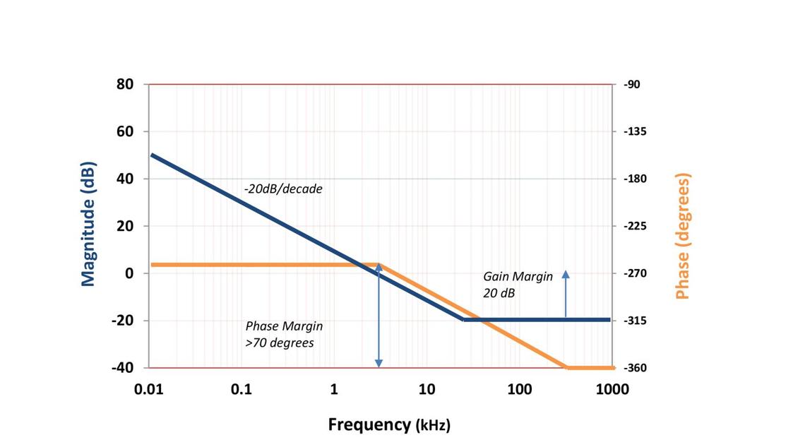
“Compensation” of the feedback signal is therefore necessary by tailoring the error amplifier frequency response to keep bandwidth high for best load-transient response while maintaining loop stability. This is characterized by a “gain margin,” typically at least -6dB, when the power train phase delay does reach -180° and a “phase margin,” typically at least 60° less than the full 360° at the frequency where gain drops to unity. Ideally, the gain should be reducing by -20 dB/decade at the unity gain point
Figure 1: Typical target control loop response
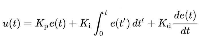
In analog compensation schemes, parallel and series resistor-capacitor networks are employed around the error amplifier to shape the feedback frequency response. These networks have “corner frequencies,” which represent “poles” or “zeroes” in the loop transfer function, which can be graphically added in a “bode plot” to give a visual indication of loop bandwidth and gain/phase margin achieved. In digital control schemes, the feedback voltage and error signal are manipulated using the logic and arithmetic functions of a processor to achieve the same effect, so it is useful to talk in terms of the mathematical representation of the desired compensation frequency response. In this case, traditional control theory can be used with a proportional-integral-differential (PID) scheme; three separate error correction signals are generated, one proportional to the instantaneous difference between the reference and the desired output, one representing the time integral of the difference or summation of difference over past time, and one representing the differential or rate of change of the error signal as an indication of its trajectory in the future. Different weightings Kp, Ki and Kd of the three PID terms can then be added, to approach an optimum loop response. The overall control function u(t) for error voltage e is then:
Digital control also allows other response compensation schemes, even non-linear, and weightings can be altered dynamically in response to changing load conditions.
The digital POLs usually have a standard configuration with a robust control loop compensation setting (PID setting) which allows for a wide range operation of input and output voltages and capacitive loads. For an application with a specific input voltage, output voltage, and capacitive load, the control loop can be optimized for a robust and stable operation and with an improved load transient response. This optimization will minimize the amount of required output decoupling capacitors for a given load transient requirement yielding an optimized cost and minimized board space. Fortunately, some suppliers provide software for this purpose. An example is the Flex Power Designer software, available free of charge from the Flex Power Modules website.
Optimizing PoL control loops with Flex Power Designer software
The starting point for loop compensation is the load requirement. A typical example is shown in Table 1 for an IC with a 1V rail.
Table 1: Typical processor IC power rail requirements
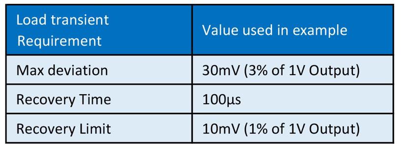
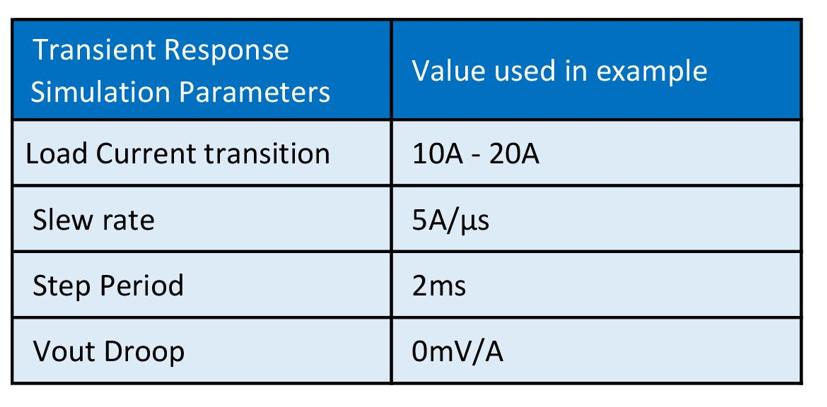
The actual load steps and the slew rate encountered depend on the application, so assumptions have to be made initially until real-life tests are conducted. In our example, the values of Table 2 are assumed.
Table 2: Transient load assumed characteristics
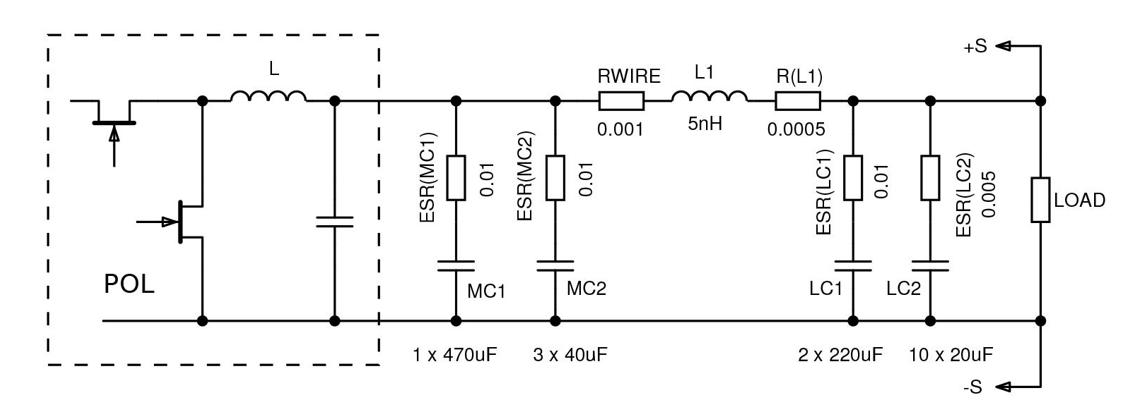
Once a PoL type is selected from the Flex range, BMR464 in this example, the components of an output filter between the PoL and load are specified. These include recommended output capacitors for energy storage, capacitors for noise filtering and any intentional or parasitic series inductance. A typical network is shown in Figure 2.
Figure 2: Typical PoL output filter network
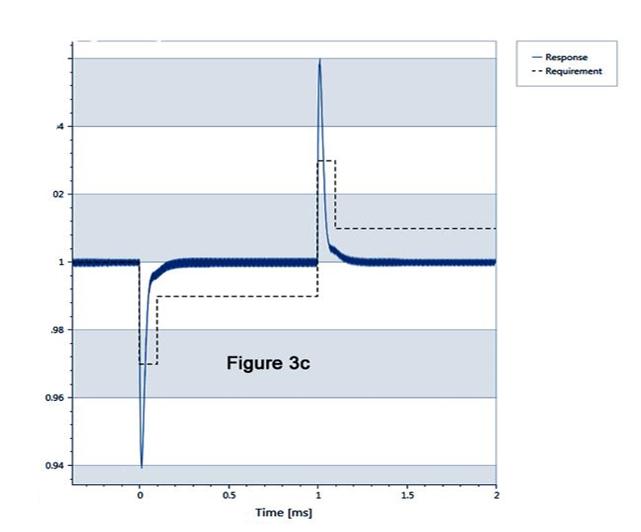
The software can apply different degrees of feedback compensation for the load network and target transient response with “robust” and “optimized” levels available. The default simulation can be plotted on a graph and typically shows a heavily damped and stable but slow response with voltage deviation above the target values, shown as dotted lines in Figure 3a. “Robust” simulation chooses preset PID weightings to improve response time to the target values but still does not achieve the voltage deviation requirements (Figure 3b). Selecting “optimized” simulation with an iterative calculation of PID weightings improves the voltage deviation and response time still further (Figure 3c). While this gives a good margin against the target voltage deviation and response time, the performance will be very sensitive to component tolerances and errors in assumed parasitic values, and could be unstable under some conditions.
Figure 3a: Robust load-transient response
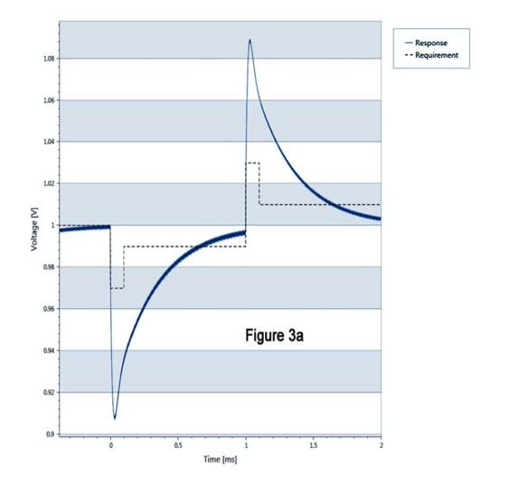
Figure 3b: Default load-transient response
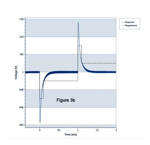
Figure 3c: Default load-transient response
Non-linear compensation response improves voltage deviation with load steps
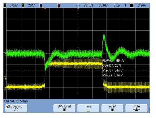
To get closer to the target specification for voltage deviation, many of Flex Power Modules’ POLs such as the BMR462/463/464/466 include a non-linear response (NLR) function. In this scheme, alongside normal PID control, the feedback voltage is monitored on a cycle-by-cycle basis and if it falls outside preset limits, the power train is set to immediately source or sink current with extra or blanked pulses respectively. This helps to correct the output deviation, effectively increasing the feedback loop bandwidth. With optimized PID and NLR control, a real-time plot of voltage deviation with the conditions defined gives Figure 4, showing recovery time well within the target 100µs with a peak deviation just a little more than our +/-30mV target at 65mV peak-to-peak.
Figure 4: Measured response of the example PoL and load system
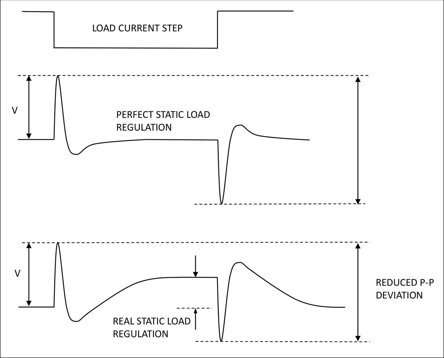
In Figure 4, the output voltage is settling to within a few millivolts of the nominal value after each load-step edge. The Flex Power Designer software allows this static regulation to be adjusted so that there is some “droop” with increasing load. This can actually improve overall dynamic regulation, as shown in Figure 5, to potentially meet the target voltage deviation specification.
Figure 5: Allowing finite static load regulation improves dynamic voltage deviation
Summary
Digital control of PoL regulators opens up a world of possibilities to optimize static and dynamic load-transient response to suit today’s demanding applications. Software such as Flex Power Designer with its user-friendly GUI makes the optimization process quick and easy.
References
[1] Optimizing Load Transient Response for PID & NLR Control: Flex Power Modules Application Note 306
[2] Loop Compensation and Decoupling Design With “The Loop Compensator”: Flex Power Modules Technical Paper 022
[3] Flex Power Designer software: https://flexpowermodules/flex-power-designer