Powering gate drives efficiently
Gate drive requirements are varied
IGBTs and MOSFETs are said to be simply voltage driven, while GaN cells are turned on with a threshold voltage but maintained on by a small current into their gate-source parasitic diode at a higher voltage - but its more complicated than that. For all devices there is a maximum voltage before stress and possible failure and there is sometimes little margin between the ideal on-voltage and the absolute maximum. Silicon carbide MOSFETs start conducting with a few volts on their gates but need around 18 V for full enhancement with an absolute maximum sometimes as low as 23 V. IGBTs and Si-MOSFETs are more forgiving with typically more than 10 V between operating and maximum gate voltage and GaN cells require a source current, strictly limited to a few mA from typically around 7 V.
Off-state voltages vary as well; while all device types are nominally off at VGS=0, they are often driven negative to offset the effect of Miller capacitance injecting current into the gate as the device switches off with high dV/dt, pulling the gate positive. A negative drive also counters the effect of any common inductance in the gate and source/emitter connections causing a transient positive gate voltage with high turn-off di/dt.
Gate drive power varies between extremes as well – the largest IGBTs may require more than 10 W because of their high total gate charge but the figure is in the mW range for GaN cells. The value depends on switching frequency and total peak to peak gate voltage swing and in practice is typically between 0.5 – 2 W for IGBTs and MOSFETs. Peak currents on the switching edges can also be in the range of amps for large devices. Gate drivers therefore need to have tight control of their output to ensure lowest conduction losses and to avoid stress and consequent unreliability. They need to have a high peak current rating and a significant continuous power rating, while operating at controlled PWM dV/dt rates for the best compromise between efficiency and EMI. They should also have undervoltage lockout and some form of detection of load faults with rapid switch-off.
Driver power rails are critical
Part of the recipe for a high-performance gate driver is the provision of its power rails, which effectively set the gate voltage levels. The voltages required such as +15/-5 V are not system standards, so a local DC/DC converter is used, powered from an available rail, typically 12 V or 24 V. The DC/DC is also normally isolated for multiple reasons: it keeps drive and load ground currents separated, gate drives are often ‘high-side’, offset from system 0 V, and in many applications, there must be agency-rated safety isolation between the switched load voltage and the controlling electronics. Figure 1 shows the elements of a typical full-featured isolated gate driver circuit and its power supply.
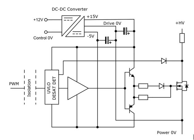
Figure 1: An isolated gate driver and power supply, here shown with rails typical for a SiC MOSFET
Low driver isolation capacitance is essential
In the high-side drive application the DC/DC and driver output ground is actually the main converter switching node which could be a high-voltage waveform at tens or hundreds of kHz with edge rates to 100 kV/µs, or conceivably more with GaN. This waveform effectively appears across the driver signal and power isolation barriers, stressing the insulation and injecting appreciable ‘displacement’ current through the barrier capacitance. For example, even a modest 10 kV/µs would force 200 mA through just 20 pF. The current then takes an indeterminate path back to its source through the control electronics, potentially causing EMI, chaotic operation and even failure of the insulation or other components.
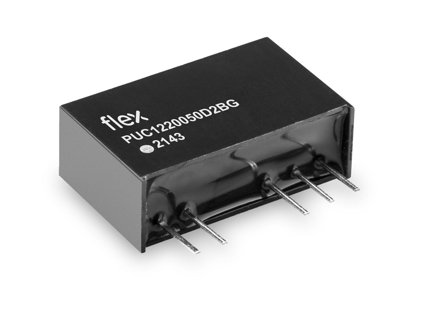
A modular solution is available for gate drive power
The need for DC/DCs tailored for gate drive power has been addressed by modules such as the PUC-2BG range from Flex Power Modules. These are 2 W parts in a SIP-7 through-hole format with industry standard pin-out. The products feature a range of fixed inputs and output combinations, suitable for IGBTs, Si-and SiC-MOSFETs and even GaN cells with further voltage and current regulation. (Figure 2).
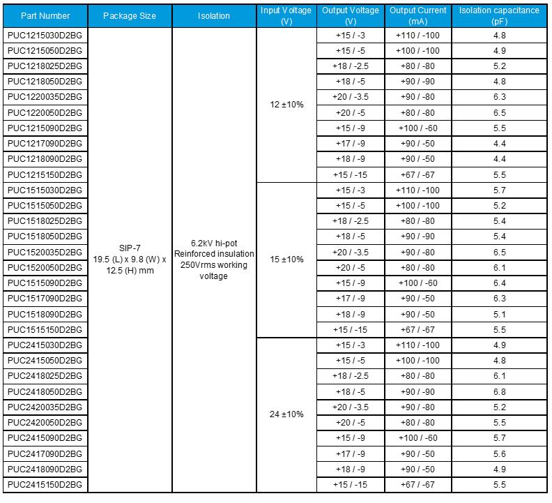
Figure 2: The PUC-2BG range of gate drive DC/DCs from Flex Power Modules for SiC/GaN/IGBT applications
A particular feature of the parts is their low isolation capacitance at 6.8 pF maximum and 4.4 pF minimum. Agency-rated safety isolation is provided, meeting the requirements of IEC/EN/UL 62368-1 for reinforced isolation with 250 Vrms system voltages and Hi-pot test voltage is 6.2 kVDC.
The parts are rugged with no derating to 85°C and operate to a maximum of 100°C. Short circuit protection is included and the outputs stay within stated specifications down to zero load, which is important to avoid transient gate overvoltages on power-up or after standby conditions, when the required gate power is close to zero and the DC/DC output might otherwise rise. Efficiency is high at typically 81% and MTBF is 13 Mhrs, for a cool-running, reliable, fit-and-forget part.